Micron Technology has picked Bechtel to build the first phase of what’s billed as the US’ biggest semiconductor plant in Clay, New York.
Bechtel will use digital-enabled construction technologies, modularisation and project controls to support time management, operations and coordination.
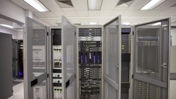
Bechtel said semiconductor fabrication is technically demanding work, requiring cleanroom systems, ultra-high-purity process infrastructure, advanced electrical systems, vibration-sensitive foundations and tightly controlled manufacturing environments.
The $100bn facility will contain up to four fabs, each with 600,000-sq-ft of cleanrooms used for manufacturing dynamic random-access memory chips for use in AI. If all four fabs are built, a quarter of all US chips will be made there.
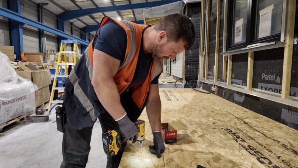
Work began in January, with Gilbane carrying out pre-construction and enabling works on the 680-acre site.
The project is due to employ 50,000 staff, including 4,500 construction roles.
It’s the biggest private investment in New York state history, estimated to add $16.7bn a year in the state’s economic output.
Craig Albert, Bechtel’s president, said: “This project represents more than the construction of a semiconductor manufacturing campus, it is part of the foundation of America’s industrial future.”
Manish Bhatia, Micron’s vice president of global operations, said: “Our New York project will be home to the most advanced memory manufacturing in the world and will serve as a cornerstone of America’s leadership in the AI era.”
Work on the project is supported by the CHIPS and Science Act which was passed in 2022, allocating $53bn in subsidies for investment in chip fabrication plants on American soil.
- Subscribe to our newsletter here to receive construction news and insights from around the world straight to your inbox
Further Reading: